MIMO Needs FinFET
7 Key Changes, Analog Designers Will Need to Make
Fortsetzung des Artikels von Teil 2
2. Use Repeatable Patterns
It is easier to deal with the complex FinFET DRC rules if the layout engineer keeps the density constant and all the devices are laid out with fixed patterns that are interrupted using dedicated ‘cut’ layers.
When applied to analog circuits, the layout regularity ensures predictable characteristic of the devices that, if implemented using an irregular layout, will deviate from the model.
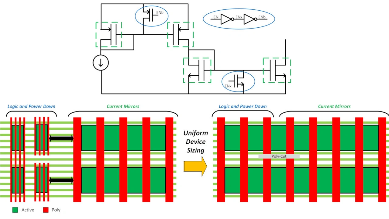
Figure 3 illustrates how this can be applied to the sizing of power down circuits in a current mirror. In a planar geometry, the designer may use minimum length devices for the power down transistors and logic and longer devices for the mirror.

Applying the same approach to FinFet creates irregular patterns for critical masks like poly and active area. The layout engineer is also forced to satisfy additional rules controlling the spacing of devices with different lengths. On the other hand, if the power down transistors use the same length of the mirrors, the layout becomes regular. This maximises layout efficiency and keeps the density of critical layers constant. Therefore, the layout engineer can create templates that can be reused for multiple analog blocks.
- 7 Key Changes, Analog Designers Will Need to Make
- 1. Do not Mix Devices Having Different Dimensions
- 2. Use Repeatable Patterns
- 3. Estimate Interconnect Parasitics From the Start
- 4. Use Digital Calibration to Correct Analog Errors
- 5. Current Density limits the Transmitter Output Power
- 6. High Flicker Noise Corner Frequency
- 7. Simulations Are Slow


