MIMO Needs FinFET
7 Key Changes, Analog Designers Will Need to Make
For analog designers, moving to FinFet technology represents a drastic change. In this article, the author present seven recommendation that should make this transition smoother and facilitate the design of high performance FinFet analog circuits.
5G terrestrial and satellite communications have already begun to use bands in the FR2 range (28–32 GHz). The range of wireless communications in these high frequency bands is limited by the short signal wavelength and these transceivers therefore rely on the integration of MIMO systems to meet the link budget and mitigate interference. For the ASIC designer, this means more channels, more radios, more digital signal processing.
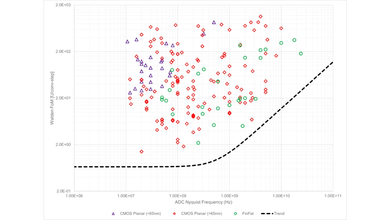
FinFet has become the ideal technology for large MIMO systems, giving high degrees of flexibility while enabling ‘digital radio’ solutions, based on RF-ADCs/DACs, that support multiple standards. There is, however, a drawback in implanting this architecture: power consumption. Figure 1 plots the energy/conversion-step of high-resolution ADCs published in the last decade. It shows that the energy-per-conversion increases exponentially when operating above 1 GHz; for example, moving the sampling frequency from 1 GHz to 5 GHz, increases the converter power by more than 20x.

Significant power can be saved by designing an RF analog front end (AFE) and thereby converting the multi-GHz RF signal to a lower intermediate-frequency (IF) below 500MHz, before performing the transition to the digital domain and relaxing the data-converters sampling frequency.
Using FinFET for analog design introduces other benefits:
- It enables compact devices,
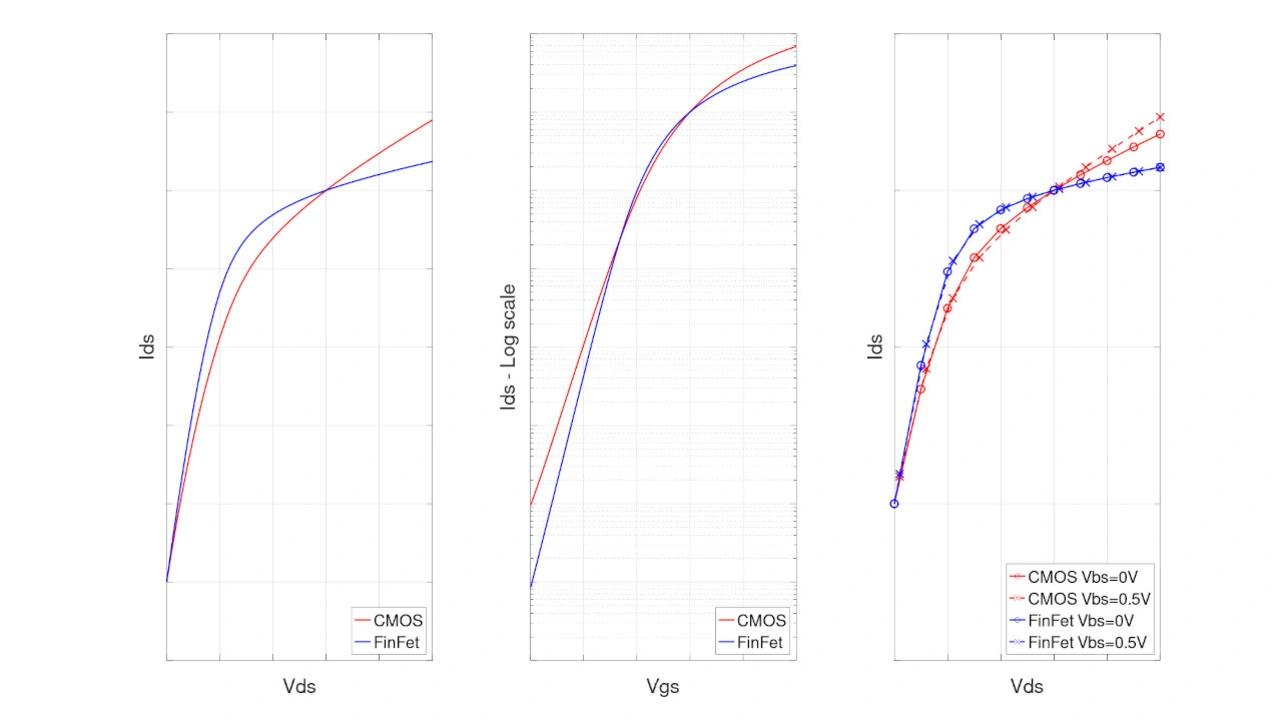
- has a high Gm and Rout,
- the subthreshold slope is practically ideal (lower leakage),
- gives excellent high-frequency performance (with peak fT of 600 GHz),
- its PMOS vs. NMOS β ratio is near 1, and
- the transistors threshold is near-enough unaffected by the body bias.

Again, there is a drawback to this approach too: the number of masks required by the technology is 2/3 times higher than planar and that makes the analog layout complicated and slow, due to the large number of design rules. This makes the technology better suited for digital Place and Route implementation, whilst using a standard ‘custom’ analog layout flow can be hard, especially using the smaller (7 nm) topologies required for these applications. So, can it be done?
Below the outline of seven rules for designing analog ICs in FinFET to make this process easier: (You can find detailed information on the seven key changes by clicking on the links provided.)
Using FinFET Technology for 5G-Systems
FinFet is the ideal technology for designing large MIMO systems: it offers small, high-speed digital signal processing to integrate flexible ‘digital’ radios. However, the expansion of RF applications into higher bands make the power consumption of RF-ADC/DAC based solutions prohibitive. Therefore, the design of low-power RF analog front-ends to convert the radio signal to lower IF frequency is paramount for the success of these systems.
The Autor

Gabriele Devita
is Director of RF/Analog/Mixed-Signal design at EnSilica. His work primarily focuses on the design of analog and digital beamforming transceivers for MIMO wireless systems, operating in the FR1 and FR2 frequency bands.
- 7 Key Changes, Analog Designers Will Need to Make
- 1. Do not Mix Devices Having Different Dimensions
- 2. Use Repeatable Patterns
- 3. Estimate Interconnect Parasitics From the Start
- 4. Use Digital Calibration to Correct Analog Errors
- 5. Current Density limits the Transmitter Output Power
- 6. High Flicker Noise Corner Frequency
- 7. Simulations Are Slow


