More diversity for new challenges
Boost for embedded computing
Fortsetzung des Artikels von Teil 1
»Tensor-Flow« as a standard

Of course, the PCI Express bus can be restricted so that existing standards can continue to be provided with new processors and peripherals. However, to make full use of the performance of new and future devices, it is time to think about new embedded computing standards. This also opens up the opportunity to dispose of a few legacy issues, for example, with I/O interfaces, and therefore to integrate new technologies – in other words, to take advantage of all the freedoms offered on the proverbial “greenfield”. For example, with COM HD, PICMG has started to work on a new high-end module concept.
The opportunities opened up by new module standards are not limited to the integration of new high-speed buses and interfaces, but also encompasses other upgrade options, for example, for mass storage. However, expansion sockets for artificial intelligence (AI) accelerators are also conceivable. The topic of AI has so far mainly been with regard to data centers and the cloud. But numerous experts are convinced that it is necessary to have the intelligence in the edge, in other words, in the embedded system on site – big data is then downstream on the next level. This means that quality at the edge is decisive – which is good for suppliers in the field of embedded computing, because the edge is typically their systems.
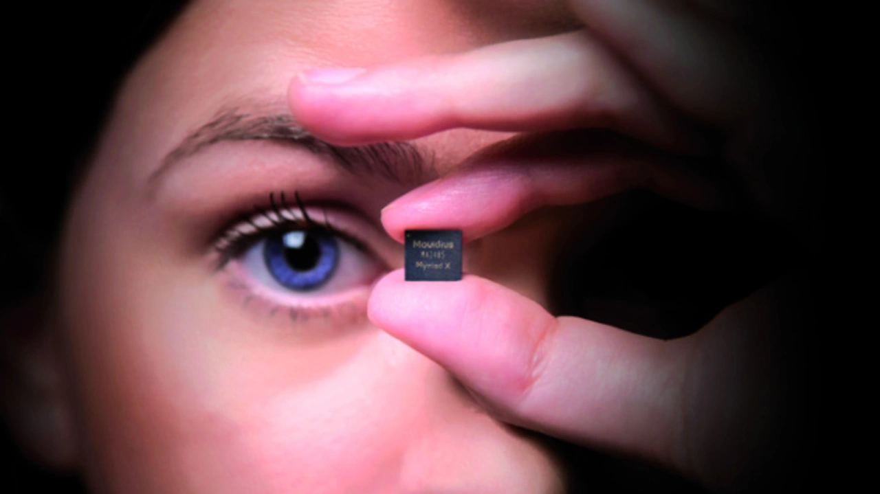
Some semiconductor manufacturers, who develop AI accelerator chips according to the basic requirements of embedded computing, also see this trend: small, low power consumption, inexpensive. Intel defines its AI accelerator “Movidius Myriad” as a vision processing unit (VPU) and thus at the same time names one of the most important fields of application: image recognition. The chip can be integrated into a USB stick, as Intel demonstrates, or as a PCI Express mini card, which Aaeon, for example, offers.
Google has also recognized the importance of the edge and developed its own Tensor Processing Unit (TPU) for this. The “Edge TPU” is an ASIC for processing “TensorFlow Lite” ML models and is designed for specific embedded requirements. Power consumption, costs and space requirements are optimized for the limited resources of edge devices. Despite the success of “Google Now”, the TPU will initially not be used in consumer devices, but in Industrial IoT (IIoT) and enterprise IoT gateways. Google therefore expects to improve reliability, security for data and devices as well as faster real-time predictions.
In addition to these AI chips, numerous others are under development, and therefore offer embedded board vendors a wide range of potential differentiating features. However, conventional components can also be used: The GPUs, integrated in the CPUs or available as stand-alone devices, also enable the acceleration of AI calculations due to their massively parallel design in a matrix structure. Some high-end GPUs even have integrated TPUs, in addition to the normal cores, for even faster calculations. Originally, these TPUs were supposed to intelligently fill gaps in the ray tracing of graphics – however, price and power requirements make the use of these devices in embedded systems rather unlikely.
Regardless of whether a new CPU architecture, PCI Express generation or AI is to be used, this means additional components that considerably expand the existing variety of boards and modules. Standardization is therefore desirable for most customers and is also, in part, carried out in the area of bus systems. Since AI in the edge is still in its infancy, standardization is difficult here, but there are already promising approaches. “TensorFlow” is on its way to becoming a de facto standard as a software tool for machine learning and AI.
And the Khronos Group, well known because of OpenCL, has developed the Neural Network Exchange Format (NNEF), to facilitate the exchange of neural networks. Users and developers of embedded systems, therefore, not only have to deal with new hardware standards, but also with new software standards – and a flood of new components.
- Boost for embedded computing
- »Tensor-Flow« as a standard


