NFC-WLC Wireless Charging Standard
Optimize Designs in the Face of Size, Cost and Performance
Fortsetzung des Artikels von Teil 1
Profound impact of RF architecture on wireless charging operation
In conventional NFC architectures, the transmitter generates a square-wave output signal (see Figure 10).
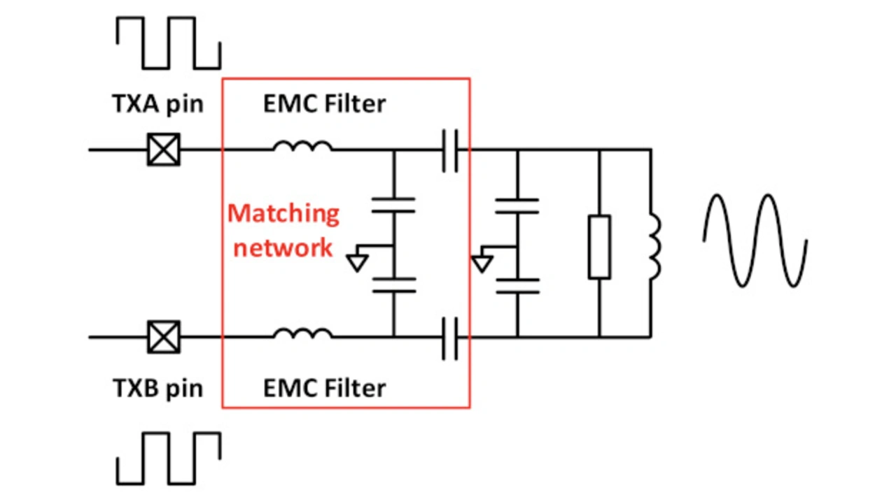
This square-wave architecture is an attractive choice for NFC component manufacturers because it is easy to implement in silicon. But the square wave output has to be shaped as a sine wave for transmission via the antenna to suppress electromagnetic emissions: this calls for an electromagnetic compatibility (EMC) filter made up of multiple external components.
In NFC wireless charging, this has two important drawbacks:
- High power losses in the poller’s EMC filter reduce the power output, and as a consequence the input power at the listener.
- The additional resonance frequency caused by the EMC filter (LC) increases the complexity of the antenna matching network, increases bill-of-material cost, and introduces additional tolerances in production.
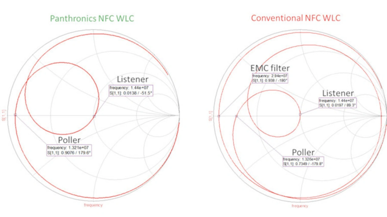
In practice, this means that the conventional NFC transmitters used in today’s wireless charging devices are limited to an output at the antenna of 1.5 W at best, and to a maximum of 500 mW at the listener: at this low power level, the time to charge a device becomes excessively long.
A different, sine wave architecture – the result of a patented silicon implementation developed by Panthronics – produces a sine-wave output at the transmitter pin (see Figure 13). As a consequence, the NFC circuit requires no lossy EMC filter, and enables a direct-to-antenna (‘DiRAC’) connection from the transmitter pin.
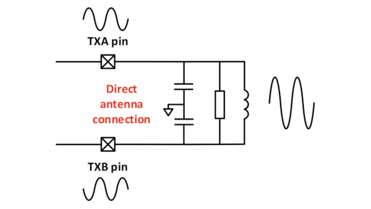
There are considerable advantages for wireless charging systems in this sine wave architecture compared to transmitters based on the conventional square wave architecture:
- Losses are reduced because the EMC filter and most matching components are eliminated.
- The reduction in component count simplifies system matching – a comparison of Figures 11 and 13 shows the much simpler matching network for the sine wave transmitter.
- The variance in performance between one production unit and another attributable to the wide tolerances in matching components is greatly reduced.
So how does this affect the three crucial design considerations described above – antenna matching, battery charge time, and size/cost?
For antenna matching, the simplicity of the matching circuit applied to the NFC100W makes configuration for specific applications much easier. In addition, the elimination of multiple wide-tolerance components means that variance in system performance over a population of production units will be far smaller.
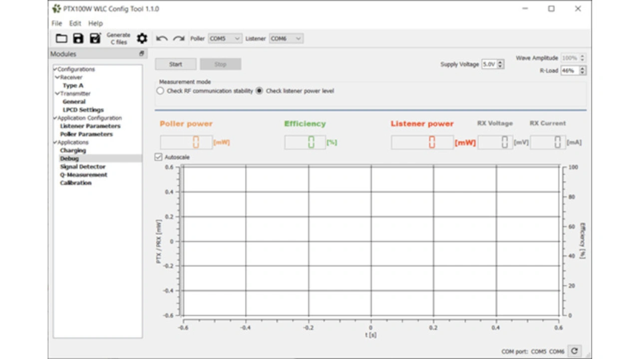
In the process for developing a poller circuit, the system designer will balance key antenna parameters such as Q factor, resonance frequency, and coupling factor, alongside physical factors such as the free area surrounding the coil, and the presence of conductive material in the vicinity of the antenna. Configuration of the antenna system is supported by the PTX100W Config tool, which allows the user to adjust various parameters:
- Power output via a programmable DC-DC converter, between 3.0 V and 5.4 V
- Amplitude of the sine wave
- the R-load used as a dummy to emulate the battery during charging
The Config tool also displays instantaneous efficiency and temperature readings (see Figure 14). By using the tool, designers can optimize received power for a specific physical arrangement of the two antennas, specified for instance as a z value for the distance between the antennas.
For any given antenna size and coupling factor, the system can be optimized, for instance, to provide maximum efficiency at a specific antenna location, or to provide a high minimum power transfer value over a large operating volume – displacement of as much as 10 mm in each direction is feasible (see Figure 15).
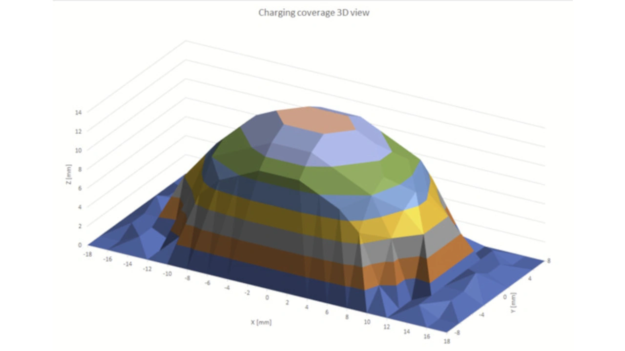
The sine wave output also allows constant optimal system matching over volume to maintain charging operation even when the poller’s and listener’s antennas are displaced from their specified positions. In a PTX100W-based system, very high sensitivity of as much as –80 dBc is possible, supporting an in-band data-transfer rate of 106 kbps for robust communication between poller and listener.
Shorter battery charging time
The higher efficiency and lower power losses of the sine wave architecture enable the PTX100W to produce a high power output at the poller’s antenna: 1 W power harvesting at the listener’s rectifier results in shorter battery charging times. The 1 W power input at the listener is around twice the level possible when using conventional square-wave architecture pollers.
A PTX100W NFC Charging Reference Design developed by Panthronics also implements an efficient rectifier circuit on the listener side.
The third of the three challenges facing the wireless charger system developer is size and cost. In the PTX100W sine wave architecture, the elimination of the EMC filter and the simpler antenna matching circuit also reduce component count, and give a board area and bill-of-materials cost saving. The system can also operate with very small antennas – a circle of diameter as small as 5 mm, and thickness of 35 µm.
Rapid system evaluation platform
Designers who wish to evaluate the performance of the PTX100W in their application environment can use the PTX100W Discrete Solution Eval Kit. This consists of:
- PTX100W poller eval board, now in version 4.0. This board includes a four-turn 26 mm × 26 mm antenna, and footprints to mount additional matching components for custom antenna designs. Low-level NFC-WLC protocol software runs on the PTX100W, and high-level protocol software on a Renesas R7S128 microcontroller.
- NFC WLC listener board, in version 6.0. This includes a four-turn 20 mm × 20 mm antenna, an Infineon SLC36 tag for NFC communication with the poller board, and a Maxim MAX77734 PMIC for power management of the on-board components and for battery charging.
- NFC WLC listener MCU board featuring a Renesas R7S128 MCU for listener system control.
Users of the eval kit have free access to the Panthronics online developer portal, and to the Antenna Config tool, enabling effective system development and optimization of power transfer operations for the requirements of the application.
The author

Francesco Antonetti
is a RF Engineer with more than thirteen years of experience in design, development, and research of RF Systems. He is experienced in performing link budget analysis and developing RF system specs and performing component level simulations for the system blocks and 3D Electromagnetic simulations.
Antonetti studied telecommunication engineering, multimedia system and telematics at the technical university of Siena, Italy. He started his career at NXP Semiconductor as RF HW application engineer. Via AMS and STMicroelectronics, he joined Panthronics. Antonetti holds three patents in the field of wireless NFC and published three technical papers about antennas.
- Optimize Designs in the Face of Size, Cost and Performance
- Profound impact of RF architecture on wireless charging operation


