Arm TechDays 2019
For Cloud and Infrastructure: This is Arms Neoverse Universe
Fortsetzung des Artikels von Teil 1
The Neoverse-E1-CPU

In addition to the Neoverse N1 CPU optimized for maximum computing power, Arm also presented a second new CPU, the Neoverse E1. This was designed for maximum data throughput in applications such as wireless/wireline points or data aggregation in a local edge network. Compared to Arms Cortex-A53, which has dominated this market segment to date, the throughput has been increased by a factor of 2.7 with identical clock frequency and production, and the computing power by a factor of 2.1. The efficiency (throughput/W) has increased by a factor of 2.4.
Although there are certain similarities with a Cortex-A55, the E1 microarchitecture differs much more from the Cortex-A55 than the Neoverse-N1 from the Cortex-A76. The most important difference is the introduction of symmetric multithreading and out-of-order command execution to capture memory latencies. In fact, cache misses dominate CPU clock cycles in packet processing. Compared to a Cortex-A55, the Neoverse-E1 reduces the proportion of clock cycles in which the CPU pipeline is blocked ("stall") in different representative workloads by up to a factor of 3.
A typical Neoverse E1 cluster consists of up to 8 CPUs, a snoop filter, up to 4 MB of L3 cache, power supply, bus interfaces to edge and cloud applications, and an accelerator coherency port (ACP, an AXI slave port) for connecting any hardware accelerators with cache stashing support.
The Neoverse E1 Microarchitecture
The E1 was presented by Sujat Jami, Senior Principal Engineer at Arm in Chandler, Arizona. Prior to Arm, Jamil spent 8 years at Marvell, where he and his team developed the Armada processors for enterprise applications based on an Arm architecture license.
From a software perspective, the two threads appear to function like two separate CPUs, i.e. the status with general-purpose registers, vector registers and system registers is replicated per thread. Each thread can therefore run on different exception levels (EL), run different operating systems, and so on. Both threads can also be executed simultaneously, i.e. instructions from both threads can be fed into the pipelines and processed in parallel (Figure 5). The computing time is allocated to the threads according to a round-robin procedure.
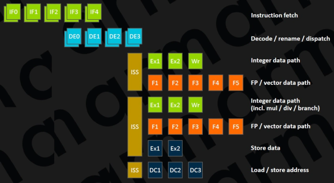
The out-of-order CPU comes with 2 command decoders and 6 execution units and has a 10-level integer pipeline (Fig. 6).

While the L1 command cache in Cortex-A53 was still working 2-fold associatively, it was changed to a 4-fold associativity in E1 as well as in A55. As usual to reduce the latency of L1 caches, the cache is Virtually Indexed and Physically Tagged (VIPT), but the L1-TLB has been increased to 15 entries and supports different page sizes. The L1 cache can be executed with 32 KB or 64 KB.
The accuracy of the jump prediction for conditional branches has been improved by the implementation of neural network algorithms. A prediction for the termination of loops has been implemented to avoid a misprediction at the end of a loop. Before the "main prediction block" for conditional jumps, so-called micro prediction blocks have been implemented whose accuracy is lower, but which can be executed several times in succession without any latency. The advantage is a speed gain due to the reduction of control flow conflicts and thus potential pipeline gaps even in small loops. Another prediction for indirect branching is only activated when needed. This saves energy as indirect branching is relatively rare.
The parity bit protected L1 data cache works like the A55 4-fold associative and completely exclusive instead of pseudo-exclusive, saving space since the data does not have to be duplicated in the L2 cache. While the A53 worked with a PIPT (physically indexed, physically tagged) cache that uses physical addresses for both index and tag, the E1, like the A55, works with a VIPT L1 data cache that uses a virtual address for the index. The advantage over the PIPT is the lower latency time, since the cache line can be resolved in parallel with the TLB translation. Of course, the tag still cannot be compared before the physical address is available. One possible problem is aliasing, which means that multiple virtual addresses can point to the same physical address. In hardware, the E1 ensures that all updates to this physical address are executed in-order by caching only one copy of the physical address at a time. While the cache on the hardware side is 4-fold associative, the software sees it as an 8-fold associative PIPT cache.
The Micro-TLB contains 16 entries and a larger memory buffer with higher data throughput in the L1 data cache increases speed especially for applications that perform numerous memory operations. The latency times for so-called pointer chasing - the reading of data via linked pointer structures - have been reduced from 3 to 2 clock cycles. In addition to the improvements to the L1 data cache itself, the data prefetcher has also been optimized. It recognizes more complex patterns of cache misses, has a larger bandwidth and can load data from L1 and L3 caches.
Full CPU Speed L2 Cache
As with the A55, the optional L2 cache per core (0, 64 or 256 KB) operates at full CPU speed. Compared to the A53, which has an L2 cache shared between all CPUs of a cluster, the latency time decreases from 12 to 6 clock cycles. The L2-TLB grew from 512 to 1024 entries because the L2 cache is now part of every single CPU. In contrast to the L1 cache, no VIPT data cache is used here, but a PIPT cache that uses physical addresses for both index and tag. The advantage is a simpler implementation and a lower energy consumption. The disadvantage of the PIPT, the longer latency time, plays a minor role with the L2 cache, since in contrast to the L1 there is enough time available to get the physical address from the TLB before the tag is compared.
While the shared L2 cache of the Cortex-A53 still worked 16-fold associatively to minimize the number of cache misses, the cache of the E1 shows 4-fold associativity like the L1. The result is a minimized access latency, which is very important for in-order microarchitectures to minimize pipeline blockages. The disadvantage is a higher probability of cache misses, which was not acceptable with the A53. For E1, it is acceptable because it still has a relatively tight L3 cache to the core, which is not available for the A53.
Finally, the separate execution units for loading and storage instructions should be dealt with again in the topic of storage systems. The common unit for both operations, the A53, turned out to be the bottleneck in the backend, which is why it was only logical to implement a second unit at the expense of power consumption and silicon area on the chip, via which loading and storage commands can now be processed in parallel. In order not to make the complexity and the described disadvantages too great, each unit is limited to one command type, so one can only execute load commands and the other can only execute memory commands.
Compared to a Cortex-A53, the memory bandwidth has increased by a factor of 4.9 with the described changes.
Optimized pipeline in the backend
As shown in Figure 6, the E1 can process 3 instructions in parallel, which are stored in a reservation station containing 8 commands. As with the A55, the E1 also has two 64-bit integer AL units that are functionally identical. This means they can perform both basic operations such as additions or bit shifts, but only one integer multiplication and integer divisions with a Radix-16 divider. This means that neither two multiplications nor two divisions can be executed in parallel, but a multiplication and an addition/bit shift operation, for example. Even if the pipeline contains 2 steps, it is important to know that many operations can be executed in only 1 clock cycle.
The two 64-bit floating point/NEON vector pipelines have their own 128-bit register set. This allows sixteen 8-bit integer, eight 16-bit integer, four 32-bit integer or floating-point operations to be performed per clock cycle with single precision, or two 64-bit integer or floating-point operations with double precision. A programmer can thus balance his application between computing power and accuracy.
With the ARMv8.2 architecture implemented in E1, floating point operations with half accuracy, i.e. 16 bit data size, were also introduced. This reduces the space required in caches and main memory, which logically increases data throughput. With the A53, it was also possible to load data in floating-point format with half accuracy, but it had to be internally converted to single accuracy format before processing, generating additional overhead and latency. The E1 can execute eight 16-bit FP16 commands per clock cycle.
In particular, many neural network algorithms use this FP16 data format to increase execution speed when training is over. In order to further accelerate these algorithms, ARMv8.2. introduced a further instruction, namely the INT8 scalar product already mentioned in N1, which combines various conventional instructions for its calculation and thus significantly reduces latency times. In concrete terms, the fact that only one instruction is fed into the pipeline instead of several, as with the A53, quadruples the speed according to ARM if the improvements in the memory system are also taken into account, even a fivefold increase. Per clock cycle, 16 INT8 instructions can be processed. Last but not least, instead of the A53's two-step multiplication addition (FMA), the E1 is executed in one step, reducing latency from 8 to 4 clock cycles.
The power consumption of an E1 CPU, including 32 KB L1 cache and 128 KB L2 cache, is just 183 mW at 2.5 GHz clock frequency and a core supply voltage of 0.75 V. The silicon area in TSMC's 7 nm implementation per core in this configuration is only 0.46 mm2.
- For Cloud and Infrastructure: This is Arms Neoverse Universe
- The Neoverse-E1-CPU
- Neoverse Reference Designs
- Neoverse-N1 Hyperscale-Reference Design
- Neoverse Development Board
- Conclusion


