Interview with Dr. Peter Wawer, Infineon
»We See Ourselves Very Well Positioned«
Fortsetzung des Artikels von Teil 2
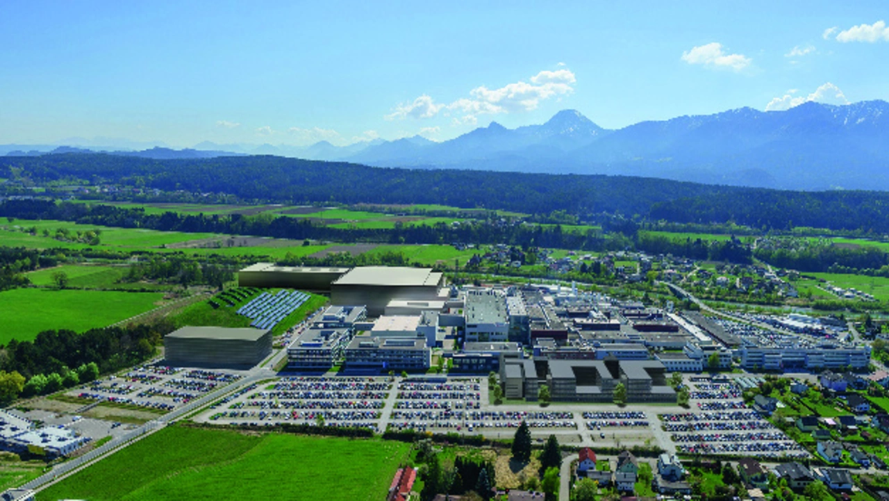
New 300-mm Fab in Villach will also benefit SiC
Although the market share of silicon carbide will increase significantly, Infineon will build a new 300-millimeter fab in Villach for 1.6 billion euros. Consequently, this is not an investment in SiC or GaN, but in MOSFET and IGBT. So the silicon power semiconductors had not come to their end yet, are they?
Dr. Peter Wawer: Absolutely not! Despite all the excitement for wide bandgap semiconductor materials – GaN and SiC – we have to admit that they are still at the beginning of their market development. Currently, global sales of wide bandgap semiconductor devices are in the hundreds of millions, while silicon devices for power electronics are worth tens of billions. Even with over-proportional growth rates, it will still take many years before wide bandgap devices will play a significant role in the power semiconductor market.
At the same time, it is also noteworthy that silicon components are also continuing to advance. Especially the production on 300 millimeter wafers results in economies of scale. So if cost plays the dominant role and not performance, wide bandgap will have no chance against silicon in the foreseeable future.

Which kind of products will then be used to fill the existing production capacities in Villach?
Silicon carbide, of course. (Laughs.) In order to increase our profitability, we will migrate the products that are still manufactured on 150- and 200-millimeter lines there today to 300 millimeters. This will free up the equipment for products that cannot be migrated to 300 millimeters in the foreseeable future due to the available wafer diameters – in other words, primarily silicon carbide and gallium nitride.
This is an integral part of our overall strategy for the site. The new 300 millimeter fab in Villach will enable us to achieve strong growth in compound semiconductors. Our new production facility is therefore a clear commitment and also an investment in GaN and SiC.
Talking of 300 millimeters: Dresden has been processing 300 millimeter thin wafers for some time now. Why did Infineon take this step and which technical challenges had to be tackled?
State-of-the-art MOSFETs and IGBTs are vertical components in order to minimize the ohmic resistance – the RDS(on). And since silicon is a relatively poor electrical conductor, this means that the thinner the better. That's why we took the bold step many years ago and migrated to thin wafers – first at 150 millimeters, then at 200 millimeters. And so it was the obvious consequence to migrate this manufacturing technology to 300 millimeters.

However, a wafer with a diameter of 300 millimeters and a thickness of less than 100 micrometers is of course much more difficult to process. In other words, the migration involved many years of research and development – both internally and together with the equipment manufacturers. And then it was necessary to get this manufacturing line up and running not only under laboratory conditions, but also in highly automated mass production facilities such as found only in Dresden and soon also in Villach.
We are quite proud that we have successfully ramped up our 300 mm fab in Dresden over the last one to one and a half years in line with market developments. There we can now manufacture all power products – MOSFETs and IGBTs. However, we have also seen that we need another location like Dresden, and our choice was Villach. Our approach there: identical. We will therefore first create the building shell and then successively equip the cleanroom area with equipment. Thus we do not have to risk spending money on non-productive equipment.
Let’s take a look into the future. How do you think the market will be split between silicon IGBTs and silicon carbide MOSFETs?
I am confident that IGBTs will grow at a single-digit rate not only for the next five years, but for the next ten. We are targeting a total growth rate of eight percent. We expect silicon carbide to grow at a significant double-digit rate. Depending on which market researcher you ask and which segment you look at, the estimates range between 20 and 40 percent. Therefore, I would rather not give an exact forecast for silicon carbide.
The forecasts also show that in a five-year time frame silicon will still dominate the market with well over 80 percent. But silicon carbide will rise from virtually zero to a market share of a low double-digit percentage. And this is a market we want to be a part of.
Dr. Wawer, thank you very much for the interview.
The interview was conducted by Ralf Higgelke.
- »We See Ourselves Very Well Positioned«
- Supply Agreement with Wolfspeed, Acquisition of Siltectra
- New 300-mm Fab in Villach will also benefit SiC


