A new approach to micro-structuring
OLED full color displays without color filter
Scientists at Fraunhofer FEP have developed a new process for micro-structuring OLEDs on silicon.
This means that there will be no need for color filters and shadow masks in the future and furthermore, the process will allow the development of full-color displays.
OLED micro displays are thin and self-luminous. More and more manufacturers are turning to OLED micro displays for applications such as data glasses precisely because of these advantages. However, the current challenge in OLED technology is that full-color displays can only be realized by using color filters or shadow masks and they in turn reduce the resolution of OLEDs.
Companies are therefore keen to try new approaches with which micro displays, which deliver high resolution as well as efficiency and durability, can be manufactured. One of the biggest problems is the structuring of organic layers in OLEDs, because conventional methods, such as photolithography, cannot be applied to organic semiconductor materials. In 2016, scientists at the Fraunhofer Institute for Organic Electronics, Electron Beam and Plasma Technology (FEP) first demonstrated their electron beam approach for micro structuring. This patented process made it possible to structure a complete OLED through its encapsulation and thus generate any structures as well as high-resolution images in grayscale.
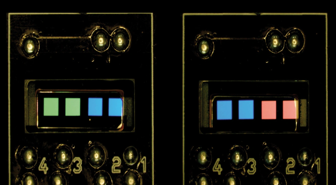
The researchers have now further developed the electron beam process, and made it possible to produce a full-color OLED pattern without a color filter. In order to produce the red, green and blue pixels, an organic layer of the OLED itself is structured using a thermal electron beam process. This structuring causes the thickness of the layer stack to change, which in turn enables the emission of different colors. This is therefore the first major step towards development of full-color displays without the need for restrictive color filters in the process. "With our electron beam process it is possible to thermally structure even sensitive organic materials without damaging their underlying layers," explains Elisabeth Bodenstein, a developer in the Fraunhofer FEP project team.
The results were obtained by simulation and initial estimation of the HTL (Hole Transport Layer) thicknesses structured with the electron beam. The researchers even achieved the decoupling of red, green and blue from the white OLED. Proof of principle at the Fraunhofer FEP enabled the scientists to demonstrate the colors with comparable OLED performance on initial test substrates. The researchers point to additional application areas such as the processing of inorganic layers, photovoltaics, production of MEMS and thin-film technology.
The next milestone: Getting established in the industry
Over the next few years, the researchers at Fraunhofer and their partners plan to develop OLED micro displays using the new process and establish it in industry through licensing. Among other things, they want to further miniaturize the structures and optimize the process. The next step is to integrate micro structuring into existing processes in order to gain know-how for, and with, industrial partners. With that, the future transfer of the test results to an existing process line is to be achieved in order to enable a later introduction of the technology at industry level.
Accompanying this are the scientists’ plans to extend the simulation of OLEDs. The color spectrum of OLEDs is to be broadened by adapting materials and layer thicknesses. Over time the use of displays in data glasses, e.g. for special applications in industry or medicine, could be enabled up by this process.


