Interview with Alex Lidow
“Now we can attack silicon MOSFETs directly!”
Fortsetzung des Artikels von Teil 1
Integration Overcomes Physical Limitations
So after looking into the past, let’s come to the future. At the technical seminar at APEC 2018 you said that integration is the way to go with gallium nitride. Why?
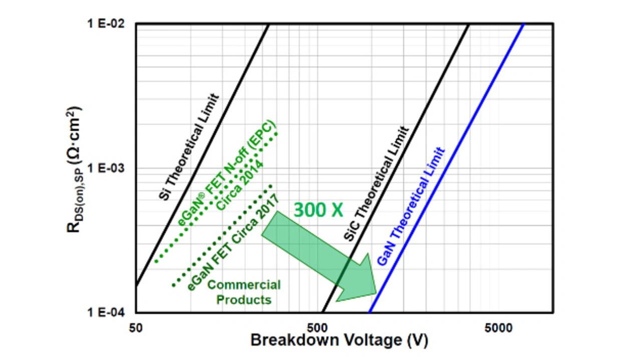
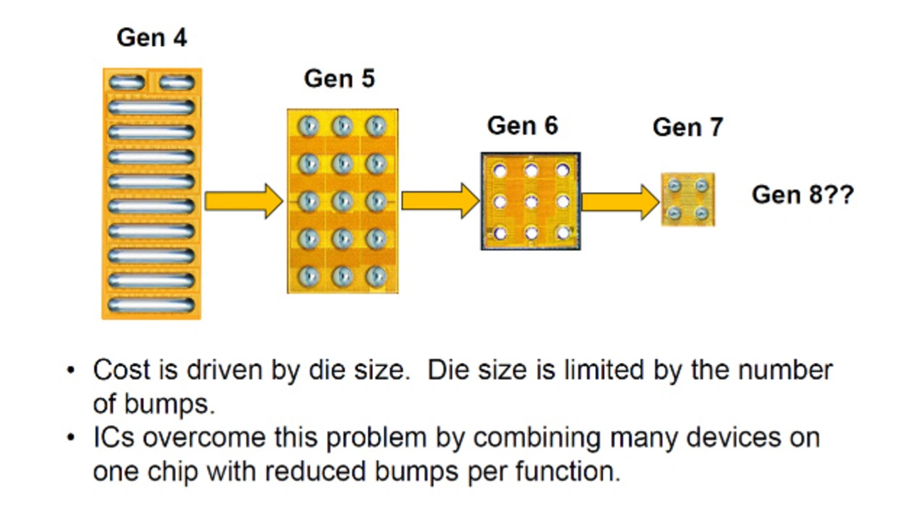
Our current Gen5 devices are some 300x away from the theoretical performance limits. So you could shrink the transistor 300 times, but then you would not be able to get the power in and out. The physical area for connecting to the PCB is the limiting factor. The only way to solve this issue is by integrating more devices and functions onto the chip.
Let’s take an example. A discrete half-bridge contains two transistors with three terminals each, so in total six terminals. But a monolithic half-bridge only has five terminals. So you save one connection to the outside. Now let’s take another example: a multi-level converter. Deployed as a discrete solution, it may need round about ten different terminals, but in a monolithically integrated device you basically have just the input, the output and the control terminal.
Is the physical area for the connections the only limitation?
Actually the physical area by itself is not the issue, but the electromigration in the interface between the printed circuit board and the GaN device. Electromigration is a well-known effect. Imagine a torrent of electrons rushing through the metal layer and bumping into the atomic nuclei, pushing them around gradually by their momentum, creating voids in the metal layer. There is a limit for each metal on how high the current density is for a given time.
With Gen5 we are at that limit right now, and with Gen6 we will go beyond that. So we are working on solving this issue. We are looking at different options like making the metal layers thicker or using heavier metals so that the atomic nuclei were not pushed around that much. But if you go for 300 times more you have to look for totally different solutions, and integration is one of these.
When we met last time at PCIM 2017 you told me that next year you will have some more ICs in place. Please tell me a little bit more on what you have achieved since then.
We have several new products; five of them are demonstration boards. These are very important to us, because they showcase how powerful our devices are. And we do all the engineering that is needed to get the most out of our devices. In March of 2018 we also introduced two integrated circuits, the EPC2112 and EPC2115. Both of these ICs incorporate driver functions on the same chip as the power transistor. In the case of the EPC2115, there are two power transistors and their drivers integrated onto a singe chip.
I remember you saying teaching engineers to work with GaN devices is like teaching a Volkswagen Beetle driver how to drive a Ferrari.
(Laughs) Absolutely! We have to provide our customers with design kits where we have done a lot of the hard work for them. So for each device our customers are immediately able to buy a corresponding design kit with all the Gerber files included.
We have a 5 phase 700 W, 48 to 12 volts demonstration board that has a power density of 1250 watts per cubic inch. We also have a smaller one with only one phase with 1400 watts per cubic inch. The EPC9204 is a point-of-load converter for 12 volts to 1 volt with a switching frequency of up to 10 megahertz.
We also have released two ICs where we integrated the driver with the transistor monolithically right onto the same GaN chip. This saves the user all the efforts of having to bias separately the driver and the switches. So now we are able to plug this chip onto a microprocessor, and a milliamp logic level signal is able to drive the power supply of the microprocessor at some 7 megahertz. Many of the issues with sensitivity to layout and parasitic inductances are solved by this approach.
My goal is integrating a half-bridge with all the drivers and level shifters monolithically. This is a huge challenge, and we are investing a lot of money into. But ultimately this may change the definition of a power component from a single transistor to a complete half-bridge with all the level shifters and drivers. Just input, output, and logic level signals for managing the component.
- “Now we can attack silicon MOSFETs directly!”
- Integration Overcomes Physical Limitations
- Monolithical Multilevel Converters will come


