Dr. Peter Friedrichs, Infineon
How to Reduce SiC Wafer Prices Faster
Infineon continuously expands its portfolio of silicon carbide devices. So we asked Dr. Peter Friedrichs, Senior Director SiC, how much progress is being made on a second generation of SiC MOSFETs and how prices for raw wafers could drop faster.
DESIGN&ELEKTRONIK: Dr. Friedrichs, what is Infineon's current focus with regard to silicon carbide?
Dr. Peter Friedrichs: Regarding products, we concentrate to continuously expand our SiC portfolio. We have established a very good foundation in silicon carbide with our first-generation trench-based 1200-Volt SiC MOSFETs. We are now expanding this significantly with regard to voltage classes and other packages. By the end of this year, we intend to offer the largest portfolio of almost 200 SiC products, if we combine discrete MOSFETs and modules as well as diodes.

From a technological perspective, we have advanced the development of a second generation of our trench-based SiC MOSFETs. Our customers have confirmed that with our first generation we have a high quality and robust product on the market. Today, we are already ahead of the competition, if you take the particularly relevant turn-on losses as the main criterion for evaluating today's SiC MOSFETs (see Fig. 1; editor's note).
D&E: What will be changing in the second generation?
Friedrichs: Up to now, SiC MOSFETs have mainly been used in specific applications, such as solar inverters or EV chargers. There is already a mass market for them. With the upcoming second generation, we expect to offer a technology that will open up many more applications for silicon carbide. Thanks to technical advantages such as a higher current-carrying capacity and a larger safe operating range, the available market will be significantly enlarged once again.

D&E: Silicon carbide is a very expensive substrate. What actions has Infineon taken to reduce these costs?
Friedrichs: Even if we see the wafer price coming down, the cost of the base material will continue to be significantly higher for silicon carbide than for silicon. This is fundamentally caused by the expensive and time-consuming manufacturing process (see Figure 2; editor's note). If you break down the costs of an electronic component, you will find out quickly that the raw wafer accounts for more than half of the total device costs. If the costs of an SiC device have to be reduced, then we have to reduce this share.
For this purpose, we acquired Siltectra in November 2018 for example. This Dresden-based company has developed a technology called Cold Split, which enables us to use raw wafers more efficiently. We have announced that we will take this technology to commercial maturity. And we have already accomplished about one third of this journey.
D&E: Could you please disclose more about it?
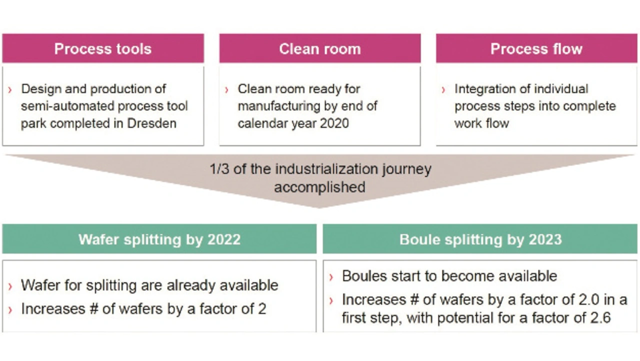
Friedrichs: Sure. When we acquired Siltectra, this start-up had an impressive lab demonstrator as proof of concept. To bring this system to an operational level so that it fits into a mass manufacturing environment, we had to develop completely new process equipment (see Fig. 3; editor's note). There was nothing to buy off the shelf. Together with proven partners, we have designed semi-automatic equipment and installed it at Siltectra in Dresden. Until the end of 2020, a new clean room will be built there. This will enable us to integrate the cold-split technology step by step into the manufacturing process for some first products.
D&E: When do you expect Cold Split to be available for industrial use and to be productive?
Friedrichs: We expect the so-called twinning to be up and running by 2022. By twinning I mean that a standard SiC wafer that has already been processed is divided into two thinner ones. The lower wafer can be processed in this way as well. Due to some developments on the raw material market we expect that in the near future the so-called boules for splitting will also become available.

These boules are the raw SiC crystals from which the wafers are sawn. If boules are available, we want to use the cold-split technology also for the so-called boule splitting (see picture 4; editor's note). This should enable us to at least double the number of raw SiC wafers we can manufacture with one boule. This separation technique – when used for both boule and wafer splitting – is certainly the most efficient way to use this very expensive raw material in the long term.
D&E: Dr. Friedrichs, thank you very much for your time.
The interview was conducted by Ralf Higgelke.
