Interview with Prof. Lorenz / PCIM
Assembly and Interconnection will be the Issue of the Future
Fortsetzung des Artikels von Teil 1
Novel Power Module Design
You said that assembly and interconnection technology would be the dominating topic of the next decade. Tell us more about it.
Prof. Leo Lorenz: With these very small and at the same time very fast switching chips, the first major challenge is to deal with this high power density in the chip package. The second challenge is to handle the extremely fast voltage and current transients, both in the module as well as in the end system.
Let’s consider the high power density in the package first. It is primarily a matter of effectively dissipating the thermal losses. In addition to the materials already known, silicon nitride, a ceramic material, is becoming more and more popular as a circuit substrate. A further aspect in the area of packaging is contacting the chip with the substrate of the module. The objective is to increase the lifetime, especially when the application has to handle many load cycles. Therefore, at the conference we will discuss various techniques such as silver sintering as well as other novel soldering techniques.
A weak spot in assembly and interconnection techniques is always the thermal junction of the heat sink to the base plate of a module. Do you see any progress there?
Yes indeed. Until now, thermally conductive pastes or foils have been used there. Over time, however, these pastes are squeezed out and leave voids, or air penetrates between the film and the heat sink or base plate. These air voids significantly increase the thermal resistance and thus limit the lifetime of the module.

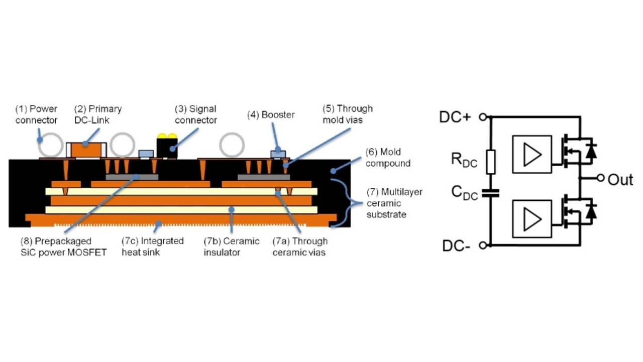
In cooperation with Fraunhofer researchers, Rogers will present an outstanding new module design with a low-inductive multilayer ceramic substrate with integrated active cooling. The switches are mounted on an insulating ceramic substrate as usual to dissipate the heat. However, a thick copper plate is placed directly underneath in order to absorb the heat and to spread it. This plate is followed by another ceramic layer for insulation. Next comes the newly designed heat sink with integrated liquid cooling, which is attached by hard-brazing. Finally the whole module is molded.
The heat sink is now part of the module housing. This eliminates the interface between the base plate and the heat sink, which is critical for heat dissipation in conventional modules. Depending on the system developer’s expertise, the thermal resistance of this interface accounts for up to 70 percent of the total thermal resistance from the chip to the heat sink, making it the most critical part of the entire system.
What about the other challenge, the fast transients in current and voltage?
There the way is to minimize the area of all the loops, in which the current commutates – mainly the so-called »hot« loop with the DC-link capacitor and the power transistors. Even here, the Rogers and Fraunhofer solution just mentioned offers a new solution. The central copper layer shown in the picture has the task to spread the heat, but at the same time to carry the current to the DC-link capacitor. The transistors are connected directly to the surface of the module. Thus not only the area of this hot loop becomes very small, but also an additional RF capacitor with a resistor can be placed close to the switches. Thereby the RF energy generated by the fast switching of the switching cell is »extinguished« locally at the same place. The large DC-link capacitor is then responsible for the real energy storage, but it is no longer stressed by the fast switching transitions.
And this approach also addresses a third issue: Due to the fast switching, the control must also be connected as short as possible to the switching cell. This new encapsulated module is connected to the top through vias, so that the control and protective circuitry can be placed close to the switches. Thus it is possible to control the switching process oscillation-free and to detect and switch off a short circuit within the shortest possible time.

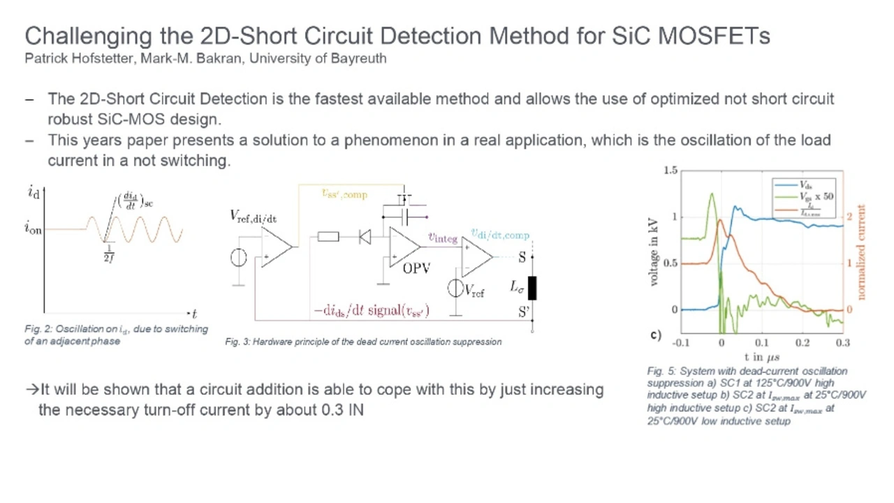
In a very interesting paper, researchers from the University of Bayreuth discuss a new concept of detecting and switching off a short circuit. Until now, the detection methods were dimensioned in such a way, that the short circuit was detected not before two to three microseconds, and switched off after about four to ten microseconds – depending on the switch technology and performance level. This is adequate for silicon transistors in conventional designs and chip sizes, but far too slow for wide bandgap switches and new fast-switching silicon transistors. As soon as the transistor is switched on – the current is still rising – it is possible to detect, whether the system is operating as normal or whether a fault is to be expected – for example, a short circuit – and the control circuit must therefore react accordingly. However, it must also be ensured, that the short circuit detection does not respond to any oscillation during the switching process. An appropriate electronic filter as to suppress all these oscillations without disabling the protection features. After all, a short circuit has to be detected reliably at all times.
In summary, we have fifty papers solely dealing with future module technologies, new materials for excellent heat dissipation with simultaneously good insulation as well as assembly and chip bonding techniques. This is the biggest single topic this year. And I am absolutely sure that this will continue for the next ten years.
The third area you mentioned is »High-Tech China«. You have lived and taught in China for many years. Recently you observed something. Tell us more about it.
The Chinese company CRRC has transferred the IGBT technology of Dynex Semiconductor [acquisition in 2008; editor’s note] to China. In the beginning this was a bit bumpy, but today CRRC has a state-of-the-art wafer fab and an excellent research institute, including a lab for power semiconductor devices. In that laboratory, a new generation of IGBTs has been developed which comes very close to what the market leaders have today.
This refers on the one hand to the high cell density in trench gate technology. In modern IGBTs, not all gates are electrically connected. Among other things, these passive gates serve to adjust the electron-hole plasma in the bulk of the silicon correctly and to manage the controllability of the transistor. The market leaders have been doing this for quite some time, but CRRC has now also implemented this in an excellent way in their lab.
On the other hand this refers to the surface metallization with thick copper layers, a step which has taken CRRC now, too. These copper layers are used as heat buffers for short overload conditions, and due to the copper wire bonding the IGBTs are able to withstand many more load cycles. This increases their lifetime up to five to ten times.
China is on the right track. I therefore still believe that we have to keep on working hard to stay ahead or at least be able to keep up. There is one thing we should not forget: If something has been proven as feasible in the laboratory in China, then the time to market for the first products based on it is usually much shorter than with us. Six or seven years ago I had already stated – and I have to repeat myself –, that Made in China 2025 has already outperformed us in specific areas of power electronics.
This is also reflected in the number of papers we received from China. At PCIM Europe there will be ten presentations from Chinese universities, research institutes and companies this year. This number has increased dramatically. At other conferences, up to 50 percent of all abstracts today originate from »Greater China«.
- Assembly and Interconnection will be the Issue of the Future
- Novel Power Module Design
- Processing on 300-mm Wafers and Special Sessions at PCIM
- Limited Availability of SiC Raw Wafers and Gallium Oxide


