Interview with Prof. Lorenz / PCIM
Assembly and Interconnection will be the Issue of the Future
The PCIM Europe will be taking place from May 7 to 9, 2019. DESIGN&ELEKTRONIK spoke with Prof. Dr. Leo Lorenz, Chairman of the Advisory Board, about the main topics of this year's conference and which issues will dominate the power electronics in the coming years.
DESIGN&ELEKTRONIK: If you take a look at the conference schedule of PCIM Europe 2019, what do you think are the main topics this year?
Professor Leo Lorenz: At the conference, we will illustrate exactly in which direction power electronics will evolve in the next several years. For me, therefore, the focus lies on three fundamental subjects: firstly, wide band gap technologies, and secondly, highly reliable embedded power integration. Ultimately, the latter topic encompasses the design of power modules for extremely fast switches, new materials for good insulation with excellent heat dissipation, and assembly and interconnection techniques. From my point of view, this will dominate the discussion over the next maybe ten years. Thirdly, one main focus is »High-Tech China«.
Let’s take a more in-depth look into these three topics. What do you think is new regarding wide bandgap technologies?
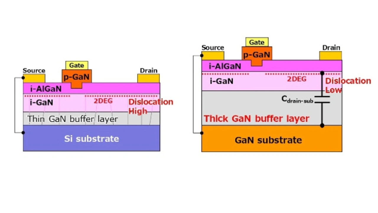
At device level, gallium nitride on gallium nitride is an interesting subject. All solutions currently available on the market use a standard silicon wafer as carrier to deposit gallium nitride on it and create the transistor. However, due to the different coefficients of thermal expansion and the different crystal structures of silicon and gallium nitride, the interface between these two materials is the weak spot. In order to overcome this, stress or buffer layers are built in as intermediate layers.

Gallium nitride on gallium nitride has not been taken seriously. Until now, this approach has been considered to be far too expensive, and the wafer diameter was limited. But Panasonic is going to show us, that GaN on GaN is economically feasible even on 150 millimeter wafers. This offers new degrees of freedom with even lower switching losses and a stable low switch-on resistance. This might, for example, reduce the output capacitance significantly, as the thickness of the material can be varied more easily. By lowering the output capacity, the dynamic losses are also reduced as well. Additionally, the turn-on resistance would be more stable, because the number of electron traps in the bulk of the semiconductor material would decrease significantly. This in turn would reduce conduction losses.
What about integration with gallium nitride?
This is also becoming increasingly important. We have a couple of papers, in which the entire control circuit, besides the power stage, was realized in GaN. Although this idea is not fundamentally novel, due to the fast switching of these transistors this topic is becoming much more relevant with respect to silicon. A completely new approach has been developed by the University of Stuttgart and the Fraunhofer Institute IAF in Freiburg. They are working on integrating the entire closed loop control system into gallium nitride. Nowadays, the power and control elements are separated on two individual chips in one package, but in future this will certainly be integrated monolithically onto one single chip.
Is there anything new to report about silicon carbide?
In this respect, I see a continuous but nevertheless substantial progress, but no dramatic leaps. Now the second generation of components is emerging.
On the one hand, we have the devices with a blocking voltage of up to 1200 volts. There the on-resistance is split into two more or less equal parts: the drift and the channel resistance. Currently, the focus lies on reducing the channel resistance. There are several interesting approaches to the so-called »channel engineering«: It involves the passivation, the thickness of the oxide layers and the trench-gate structures, while considering the control of the electric field strength in the cell and edge structures.
On the other hand, one trend in silicon carbide leads to higher blocking voltages. We will see some new approaches at the conference. A SiC device for 3.3 kilovolts and 1000 amps with a sintered copper chip surface for excellent short-term overload behavior and many load cycles will be presented. Taking the example of a SiC switch for ten kilovolts, the challenges of the necessary insulation techniques combined with good heat dissipation will be demonstrated. And for medium-voltage applications, a SiC switch in a cascaded topology and its dynamic behavior will be presented in detail.
However, it is important to note, that, in addition to the wide bandgap technologies, there are a number of important advancements with silicon devices. At PCIM, for example, new approaches will be shown for reverse-conducting IGBTs and specifically optimized IGBTs for e-mobility or multi-level topologies for renewable energies; their electrical and thermal behavior will also be discussed.
- Assembly and Interconnection will be the Issue of the Future
- Novel Power Module Design
- Processing on 300-mm Wafers and Special Sessions at PCIM
- Limited Availability of SiC Raw Wafers and Gallium Oxide


