Interview with Prof. Leo Lorenz / ECPE
"New Failures keep on popping up"
Ruggedness and reliability are recurring issues in the area of power semiconductors. This has not only to do with the new wide-bandgap materials. Silicon also faces these same issues over and over again. DESIGN&ELEKTRONIK asked Professor Leo Lorenz, the chairman of the ECPE, about this.
DESIGN&ELEKTRONIK: Professor Lorenz, in the preparatory discussion you said that ruggedness and reliability are currently the most discussed issues for power semiconductors. Why is that so?
Prof. Leo Lorenz: We have observed that at some conferences a major part of the submissions focuses on ruggedness and reliability of power electronic components – mainly power semiconductors – but also at system level. For this reason, we organized a workshop in mid-January 2020 within the ECPE (see [1]; editor's note). For wide-bandgap switches, we still miss some basic data on long-term stability and the basic understanding of the failures and their causes, in other words, the failure mechanisms, especially if the switches are operated at peak load conditions.
It should be taken into account that wide-bandgap semiconductors can switch extremely fast, in other words the changing rates of current and voltage are extremely high. Additionally, high electric field strengths in the cell structure have to be controlled in both blocking and on-state conditions. For these reasons, and because of the smaller chip areas and harder semiconductor material compared to silicon components of equivalent performance, it is necessary to find new approaches in packaging and interconnection technology as well as in thermal management.
This may be one of the fundamental reasons why the development cycles take much longer there, since the developers would like to see the results of field tests to better estimate the long-term service life. This is especially true for applications in solar inverters, traction drives for e-mobility – in automotive as well as in trains – and in the entire area of power grids. System developers in these sectors have to guarantee the long-term stability of the inverters and thus perform their task with great care and respect – and sometimes even with a bad gut feeling, as there is simply insufficient data available regarding long-term service life.
Are there no more unanswered questions about the ruggedness and reliability of silicon?
Prof. Leo Lorenz: Absolutely! Silicon MOSFETs and IGBTs are being pushed further and further to their physical limits. And thus, the questions of ruggedness and reliability arise anew.
Can you give us an example?
Prof. Leo Lorenz: Just recently, in the ECPE working group AQG 324 (Automotive Qualification Guideline 324, editor's note) for the revision of the "Qualification Guideline for Automotive Power Modules", we have found that failures occur in the HV-H3TRB test (High Voltage, High Humidity, High Temperature, High Reverse Bias, editor's note). This failure did not occur in the past because this test was performed at 80 volts by default for all power modules, regardless of their blocking voltage. Thus, a 1000 volt switch was tested at only 80 volts, because otherwise the losses would have been so high that no more moisture could condense on the component. Meanwhile this has changed. For the new generations of components, the moisture tests are conducted at 80 percent blocking voltage. This test is even more important for traction drives in trains, where high-blocking components are used.
New failure mechanisms became apparent which were previously not addressed by the test specification, weren’t they?
Prof. Leo Lorenz: Absolutely. The discussion about these failure modes, and how to tackle them, is going on. But a new test regulation, to carry out humidity tests at 80 percent or even at 100 percent nominal voltage, will come. The automobile and train manufacturers will insist on this, because it reflects their realistic use. For example, a 3.3 kV module will not be operated in trains only at 80 volts!
And this is only one issue among many others which are currently being discussed passionately at such workshops. There we are working on the guidelines for such test specifications. But the concern not to find failures remains. Even today, not all failure mechanisms are identified, especially when the components are optimized for specific applications and operated up to their limits.
But in order to obtain the necessary field experience, semiconductor manufacturers may have no other choice but to deliver products that may be subject to complaints after only a few years.
Prof. Leo Lorenz: Well, I think you have to swallow this bitter pill. I once experienced this first-hand when we started to deliver the first SiC Schottky diodes at Infineon in 1999 and 2000 in high volumes to a world market leader in power supplies for notebooks and consumer electronics. A large number of these power supplies were immediately returned to us as defective. You can certainly cope with the few million dollars fine, but restoring the bad image was a huge effort.
However, power semiconductors based on silicon also do not stand still. What is happening in this area?
Prof. Leo Lorenz: You're right. At the moment, MOSFETs and IGBTs are being optimized for the application. This means that entirely new voltage classes are being offered, for example 2.3 kV. Years ago, nobody wanted to buy any of these, but for solar applications with 1500 Volt DC, this is the perfect voltage. The same is now happening in the automotive sector, where 750 volts is going to be the standard. But this again raises the question just discussed regarding the ruggedness and reliability of the components. The possibilities of silicon are being exploited much further. And this may unexpectedly trigger failure modes that were previously unknown.
One topic that is discussed frequently with silicon carbide is: Should I choose trench MOSFETs or planar devices? Trench has its advantages, but also a problem with the gate oxide, hasn't it?
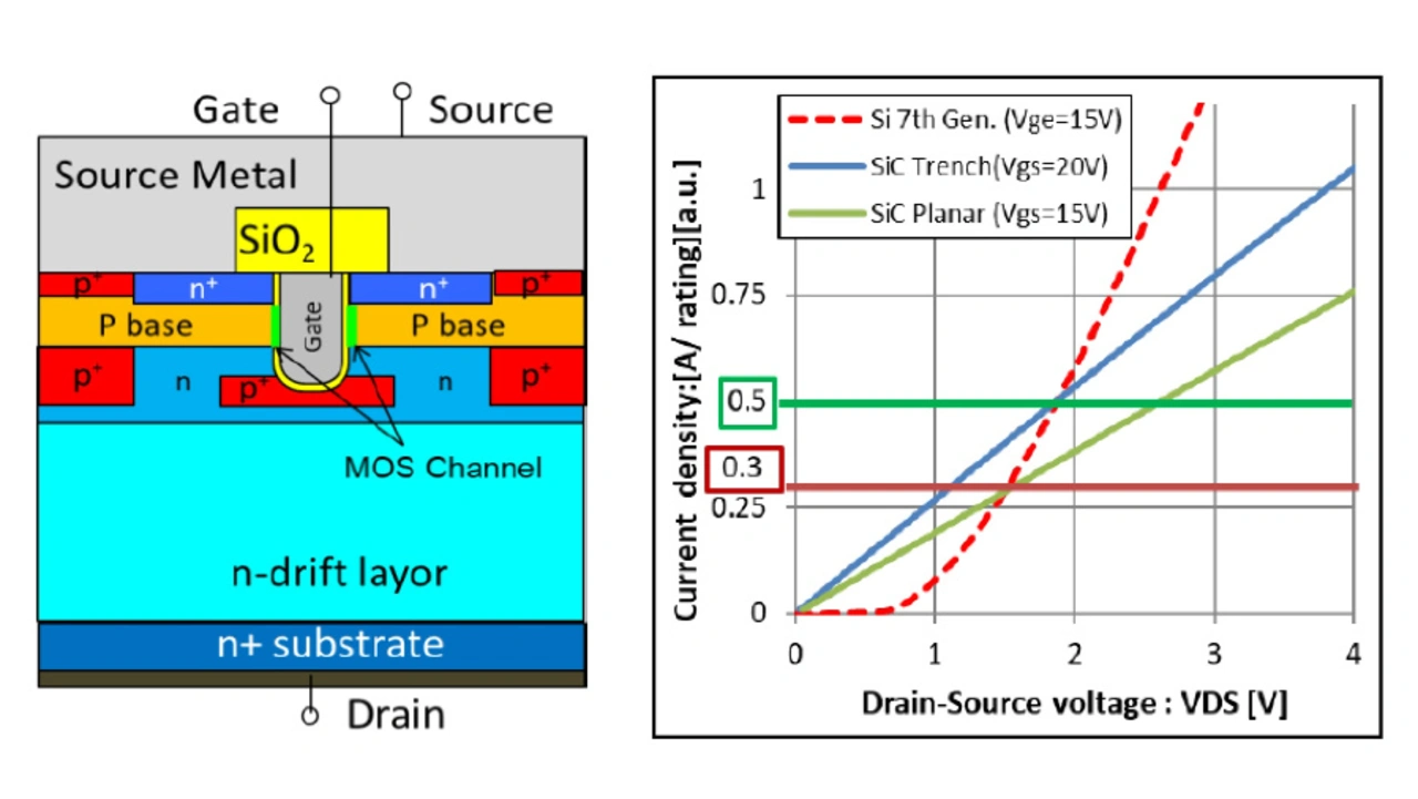
Prof. Leo Lorenz: Generally speaking, that's not true. The following applies to both cell structures: On the one hand, the high electric field must be selectively reduced at the edge structure and on the other hand, the gate oxide has to be protected. At the interface to the oxide, the electric field strength of silicon components is in the kilovolt range, while for SiC components it is in the megavolt range. At almost the same oxide thickness - in fact, it is significantly thinner for SiC components - this would significantly reduce the lifetime of the oxide. The main difference between trench and planar MOSFETs is that in the case of the trench MOSFET the critical point is at the lower edge of the trench, while in the case of the planar DMOS switch it is in the middle of the cell. In both cases, deep p-doped regions are required to keep the electric field away from the oxide.

If the MOSFET is on, the on-resistance should be as low as possible. As a matter of fact, in today's SiC MOSFETs up to about 1200 Volt blocking voltage, almost half of this on-resistance is determined by the channel. For this reason, it is important to minimize the channel resistance. In the case of trench MOSFETs, this can be achieved by the device structure. With planar D-MOSFETs you are more limited. This is why some manufacturers suggest a higher gate drive voltage – even 20 volts instead of 15 volts (see Fig. 1, editor's note). Although a higher field in the oxide is related to a lower channel resistance, it can also reduce the lifetime of the gate oxide.
The material, the thickness and the processing of the gate oxide consequently play a major role in determining the channel resistance and the life time of the device. Also, it has to be considered that the thickness of the thermal top layer of the oxide depends on the crystalline plane. So there are only advantages to driving SiC MOSFETs with higher gate voltage at first glance: Faster switching reduces the switching losses, a lower on-resistance reduces the conduction losses. But what about the expected lifetime of the gate oxide?
Some manufacturers indicate in their data sheets that their SiC MOSFETs are capable of being operated with 20 Volts. The key question here is: What is the long-term lifetime of these transistors? Nobody is able to answer that today.

Are these the only issues with the gate oxide?
Prof. Leo Lorenz: No. There are also issues in the blocking state, because the dielectric has to absorb three megavolts per centimeter. For comparison, with silicon it is only 200 kilovolts per centimeter. For this reason, the gate oxide needs to be protected, especially in the case of trench MOSFETs. Different manufacturers have developed different approaches to achieve this to better distribute the electric field and prevent that the field is concentrated at the corners of the gate oxide, for example (see Figure 2; editor's note).
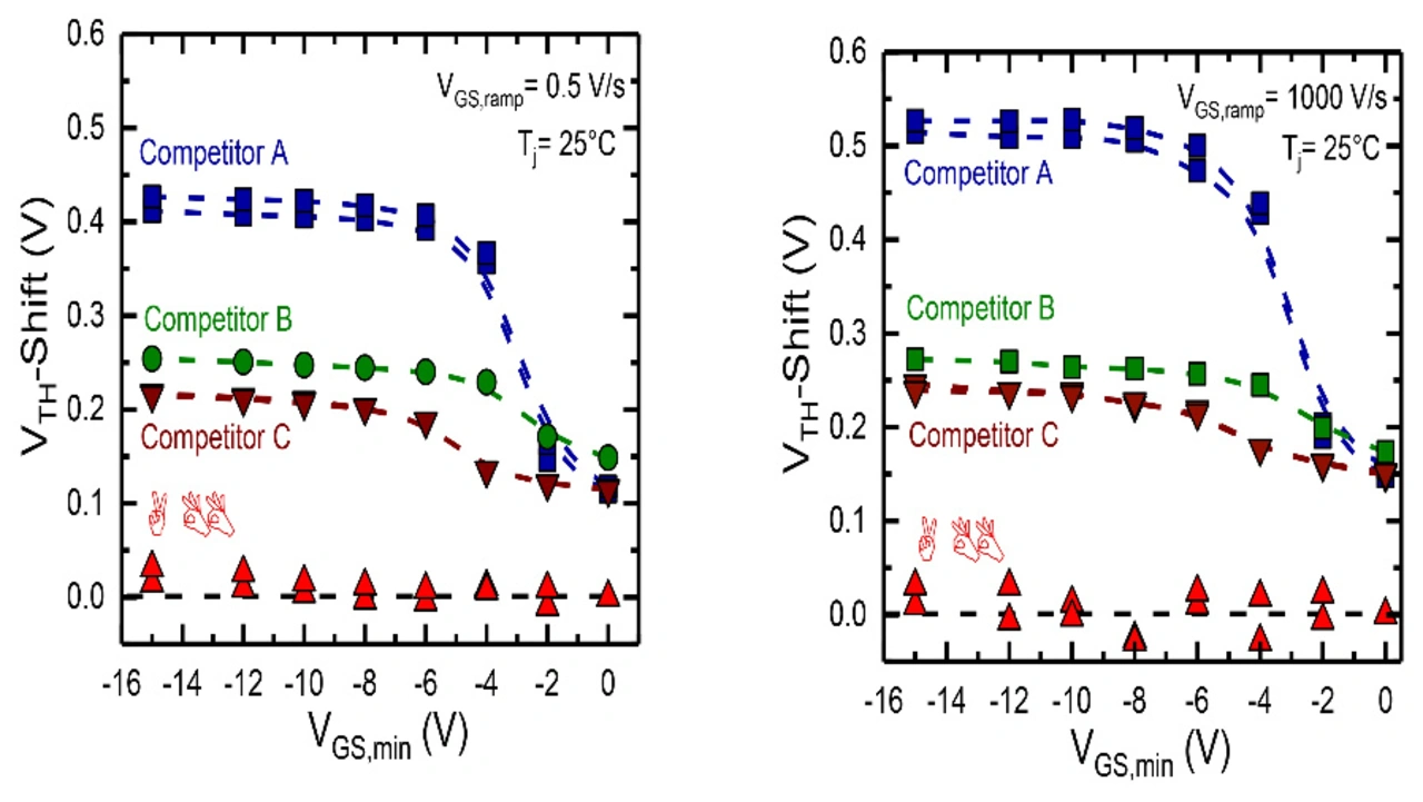
The stress from the high electric field let the threshold voltage drift upwards over time. This obviously deteriorates the on-resistance over time and thus increases the losses in the component. At the same time, it must also be considered that the threshold voltage decreases when the component becomes hot.

What are the possible ways of dealing with this?
Prof. Leo Lorenz: ABB, for example, proposes a gate oxide with a high dielectric constant. But such a gate oxide is not easy to process. But ABB achieves - or so they claim - that the threshold voltage remains constant (see Figure 3; editor's note).
However, its downside is that the temperature dependence of the operating voltage is higher. But if the operating voltage continues to drop, some claim that a normally-off component becomes a normally-on component. This is something that still has to be discussed.
Doesn't this also increase the likelihood that the upper switch will experience a parasitic turn-on in a half-bridge configuration?
Prof. Leo Lorenz: Absolutely!
Professor Lorenz, thank you very much for the conversation.
The interview was conducted by Ralf Higgelke.
| References |
|---|
| [1] Video with Prof. Nando Kaminski (University Bremen), Elektroniknet |


