Rapid Prototyping
From the Circuit Board Copy Router to the Picosecond Laser
Nobody would have thought that a simple mechanical process would one day develop into a technology that can create micrometer-fine structures on almost any material. A journey through time.
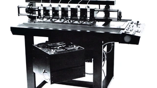
In 1975, the german engineer Jürgen Seebach developed a mechanical process for the production of printed circuit boards – the basis for the success of chemical-free printed circuit board structuring. With a circuit board copy router, drawings were transferred from paper to a copper-coated circuit board material. Further printed circuit boards were created by tracing the contours. Later, up to six printed circuit boards were manufactured in one step with a system of mechanical articulated arms and milling spindles – assuming a steady hand.
At the beginning of the 1990s, the drive technology was able to position the drive spindle automatically. The milling head was motorized in a straight line from one position to another. A milling line was created when the milling head was lowered, but not, when the milling head was raised.
Also today conductive tracks are priduced by negative structuring. But what has changed since then?
- The structuring head travels on curved paths. The track width/distance is in the range of a few microns.
- Current LPKF circuit board plotters have up to 20 tool positions and change tools independently.
- A milling depth limitation ensures the exact width of the milling contour with conical tools.
- Vacuum tables hold flexible material securely in place.
- A fiducial camera recognizes the position of the material and ensures that the individual layers fit exactly, even with multilayers.
- The LPKF CircuitPro system software reads CAD layout data and uses it to generate optimal processes, also with the help of comprehensive material and process libraries.
The range extends from the simple LPKF-E-line to the high-performance systems with a spindle speed of up to 100,000 rpm in an attractive protective housing. Mechanical systems achieve a pitch of 100 µm / 100 µm track width / spacing and a resolution of just 0.25 µm. They meet the challenges for high-precision RF circuits and can also edit single layers for multilayers.
In the early 1990s, laser systems could be used in electronics production to cut solder paste stencils. Some times later such compact laser systems were used for PCB prototyping, too. They fit through any door on rollers and only require a power connection, compressed air and dust extraction.
Printed Circuit Board Processing Machines
With special laser configurations, new areas of application have emerged in the laboratory. UV lasers structure, drill and even cut fired ceramics or thin, double-sided coated flex materials. Picosecond laser sources also process sensitive materials without thermal stress on the substrates.
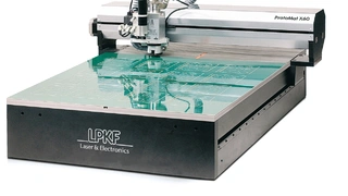
The top-of-the-range system for the electronics laboratory is the LPKF ProtoLaser H4: a high-performance spindle and six tool positions handle the mechanical processing, while an integrated laser tool is used for structuring.
A long way from the first circuit board copy router. Today, LPKF systems are widely used in PCB prototyping and provide valuable services for demanding development tasks in laboratories.
The Author

Malte Borges
since 2008 technical editor for laser technology and PCB prototyping. He accompanies chemistry-free prototyping with mechanical and laser systems and has numerous publications in trade magazines and book projects to his credit. He currently heads the Types & Bytes editorial team – specializing in technical editing.
mborges@types-bytes.de
