GaN HEMT in class E power amplifiers
Charging the wireless way
More efficiency, shorter time to charge, higher power density – those are the customer demands of semiconductor devices for wireless charging systems. A GaN HEMT can do the job in class E RF power amplifiers.
Wireless charging technology has existed for some time but only in recent years, with the proliferation of inductive wireless charging technology, become more widespread. But to make wireless charging truly ubiquitous and offer improved end-user convenience like improved freedom of positioning, it needs to evolve further, and likely will apply magnetic resonance technology over time. For the latter, high transmission frequencies (multiple MHz) are required and pose significant challenges to standard silicon power technologies within transmitter and the receiver devices.
In this article the authors introduce the benefits of GaN power devices in class E radiofrequency power amplifiers as used in wireless charging, highlight the advantages of GaN HEMT devices over MOSFETs in this power amplifier topology that is – besides class D – proposed for wireless power transfer according to the baseline specification of the Air Fuel Alliance.
Currently most wireless charging systems are based on the inductive (Qi) standard, operating by coupling at frequencies in the 100 to 300 kHz range. Although this is the more widely adopted approach, it allows charging of a single device only that needs to be placed very close to the charger in a specific orientation. Alternative topologies have gained increased attention – such as class E – to enable more free designs in wireless power transfer through resonant coupling. We have to note here that these topologies are not new, and are already used successfully in RF applications where the terminology “amplifier” is widely used to describe them. With these topologies high efficiency can be achieved in the range 1 to 10 MHz of operating frequencies. These power amplifiers are employed in the transmitter section of a wireless power system, as shown in Fig. 1.
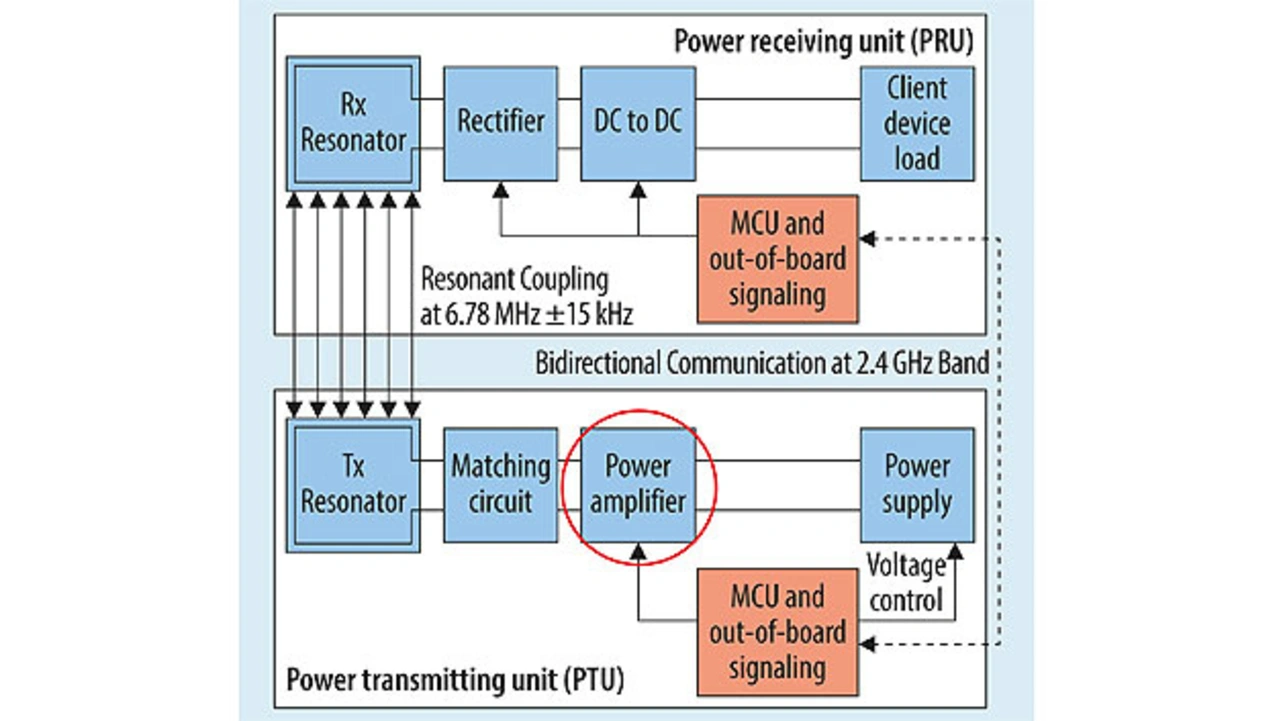
In resonant wireless charging, based on 6.78 MHz as proposed by the Air Fuel Alliance, resonant inductive coupling is used in which high-Q factor resonators enable power transfer over much greater distances using the much weaker magnetic fields in the peripheral regions. Thus, the resonant technology allows for a “drop and go” near-field charging experience, and offers considerable user experience benefits over inductive solutions.
Faraday’s law states that an electric potential is generated by a coil of wire when the magnetic flux enclosed by it varies. In wireless power transfer an RF power amplifier drives a power transmitting unit (PTU) consisting of a coil in a tuned circuit to produce a varying magnetic flux. Tuned to the same frequency, also a coil in a circuit can be found in the power receiving unit (PRU), intersecting the magnetic field so that a voltage is induced. This voltage depends on the rate of change of flux and number of turns. Output from the receiver coil is rectified and converted to the wanted level for the portable device being charged. Coupling depends on separation between the two coils, defined by the coupling factor k. A k of less than 0.5 represents a loosely coupled system as used in magnetic resonance coupling. Fig. 1 shows the system blocks of the PTU and PRU where microcontrollers with Bluetooth communication are used to request and regulate the amount of power transmitted as required by the devices being charged.
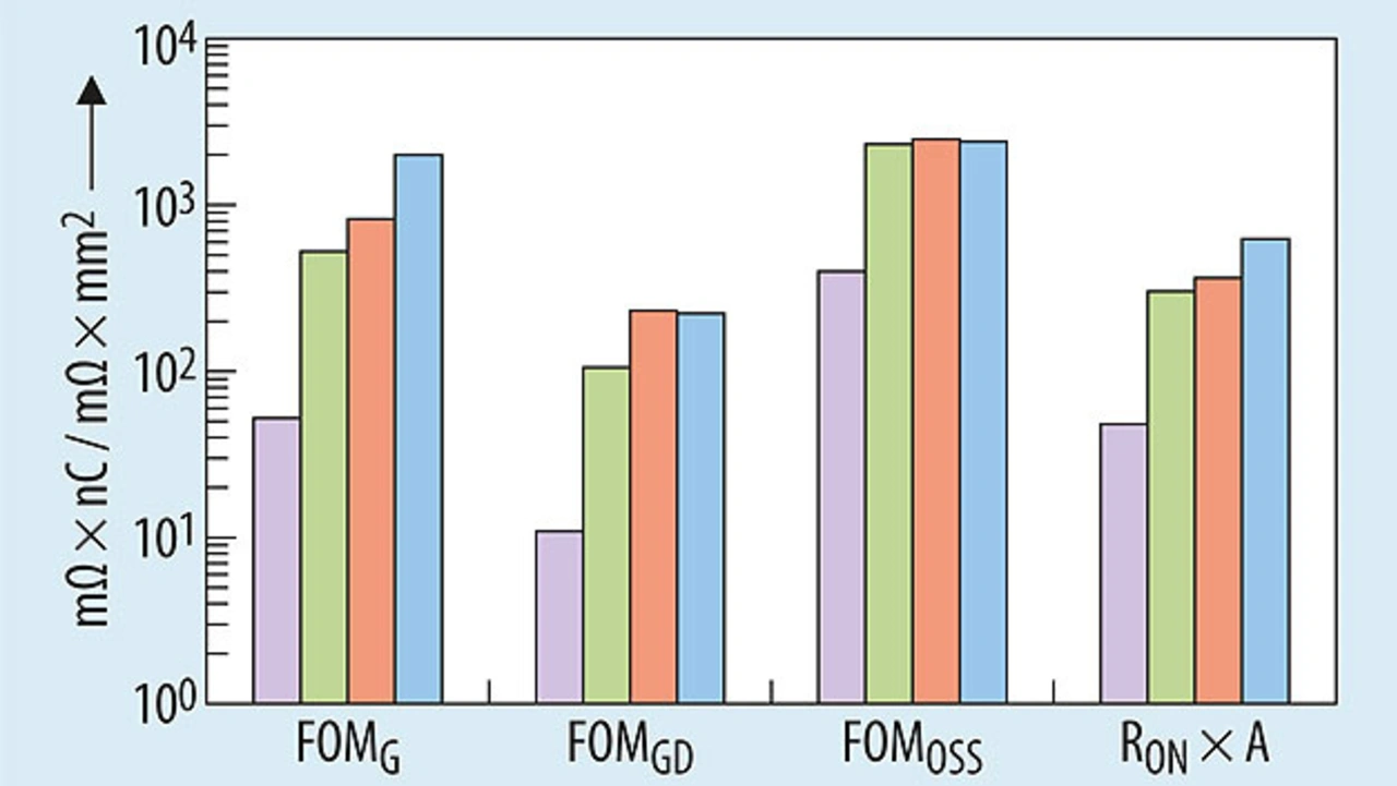
Why consider GaN for power applications including wireless charging? The merits of the relatively new GaN technology have already been proved in RF systems. Now, as significant improvements in its figure of merit (FoM) have been achieved, GaN is gaining attention for many power applications.
Fig. 2 shows the improvements presented by GaN technology compared to state-of-the-art silicon solutions from different vendors. The logarithmic scale helps to understand the quantum leap that GaN technology is offering, almost one order of magnitude for all FoMs.
Requirements of class E power amplifiers
The single-ended class E RF power amplifier topology consists of an RF inductor L1, which supplies an approximately DC current to the switching FET Q1, resonant circuit and load – as shown in Fig. 3. Q1 switches at 6.78 MHz with a fixed 50 percent duty cycle. When the circuit is tuned to the same frequency a half-sinusoidal voltage appears at the drain, which peaks at 3.56 times the DC input voltage VIN and falls back to zero just before the start of the next switching cycle, thus operating with zero voltage switching (ZVS). The load impedance must be purely resistive to enable this. An impedance matching network is placed between the power amplifier and the transmit resonator designed to cancel out all reactive elements.
The values of L2, C1 and C2 are determined according to the resonant frequencies of the two switching states. When the switch is off, C1 in parallel with the drain-source capacitance of Q1 contributes to the higher resonant frequency. When it is on, the lower resonant frequency is determined by L2 and C2 only. For ZVS operation the switching frequency must lie between the higher and lower resonant frequency, and the sum of the periods of one half cycle of each resonant frequency must be approximately equal to the period of the switching frequency.
If circuit resonance is higher than the switching frequency, the drain voltage rings to a higher peak, which can be up to seven times VIN, and will fall to zero before the start of the next switching cycle so that body diode conduction occurs during the intervening period. If on the other hand the circuit resonance is lower than the switching frequency, the drain voltage will not be zero at the start of the next switching cycle. This creates hard switching with very high associated losses at 6.78 MHz.
Requirements of class E power amplifiers, Fig. 3-6
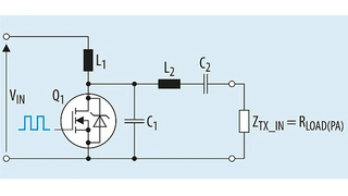
To attain high power amplifier efficiency the circuit must be correctly tuned. In addition the output current should not be too high since this creates power loss in L2 resulting from conduction and eddy current losses due to the skin effect, which are significant at 6.78 MHz. The PRU and impedance matching network should then be designed to develop a high ZTX_IN for the power amplifier load.
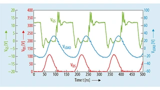
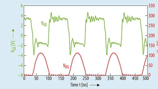
GaN technology also provides unique benefits for designs based on a class E power amplifier. One rated up to 16 W was tested using a BSC12DN20NS3 200 V, 125 mΩ OptiMOS 3 switch. To evaluate power amplifier performance and efficiency a resistive load was used and measurements taken at 25 Ω, 15 Ω and 5 Ω. Efficiency was measured at 91 – 92 percent in each case. The operating waveforms for 25 Ω are shown in Fig. 4. The red trace shows the drain voltage waveform. It is observed that the shape is not a pure half-sinewave, displaying a reduced slope at lower voltages, which prevents it from falling all the way to zero before the next switching cycle resulting in some hard switching. This effect is caused by the effect of the MOSFET COSS on the upper resonant frequency of the circuit. In silicon MOSFETs COSS increases considerably at lower voltages, which creates this distortion. Although the circuit is able to operate with acceptable efficiency and the switching losses caused by the small amount of hard switching are not high, this is still problematic. The circuit has to be retuned, resulting in a higher peak voltage, which reduces the maximum power capability and output impedance range over which the power amplifier can operate without reaching the MOSFET avalanche rating BVDSS.
A GaN HEMT with the same BVDSS and RDS(on) ratings was also tested in the same circuit, the results are shown in Fig. 5. Fig. 6 compares COSS characteristics for the two power switch types plotted on a logarithmic scale, revealing that the increase in the GaN device is much less than in the MOSFET, though the data sheet value at VDS of half BVDSS is very similar.
The drain waveform for the GaN-based device is seen to be much more sinusoidal than in the MOSFET example. Hard switching is not present, and the peak voltage is equal to 3.56 times VIN, indicating that the circuit is operating at a theoretical optimum. This allows operation over a wider range. Furthermore, in practice the circuit is easier to tune and less prone to drift caused by tolerance and temperature.
- Charging the wireless way
- Decisive GaN characteristics for wireless systems


