Dr. Thomas Reisinger, Infineon Austria
»300 Millimeter is Coming Home«
Fortsetzung des Artikels von Teil 1
Roadmap for Manufacturing Expansion
Manufacturing of power semiconductors on 300-mm wafers is gaining momentum. How many more MOSFETs or IGBTs fit on a 300-mm wafer than on a 200-mm wafer, which has been standard up to now?
Compared to the 200 mm wafer, the diameter of a 300 mm wafer is 50 percent larger, so that 2.25 times more chips can be fabricated per wafer. Depending on the complexity of the chip, this means several hundred up to 100,000 chips per wafer. But what makes the manufacturing of power semiconductors unique is the thickness of the wafers: For the manufacturing of power semiconductors, we use wafers that are only about 40 micrometers thick. To put this in perspective, standard writing paper is almost three times as thick with a thickness of 110 micrometers.
Over the next few years, production is to be successively ramped up. Please tell us a bit about the roadmap for this.
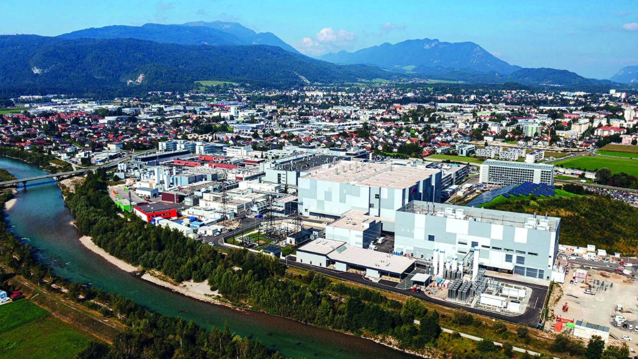
Over the next approximately four years, we want to successively bring more and more equipment into the fab so that it will be fully equipped by the end of this time frame. After all, we're talking about a gross floor area of around 60,000 square meters, which is equivalent to about 8.5 soccer fields! We also need personnel to operate the equipment. We have already been able to recruit more than two-thirds of the 400 additional vacancies for highly qualified specialists that we need for this purpose.

By how many percent has the new fab increased Infineon's production capacity in the area of power semiconductors? By how many percent will it be when the fab is fully ramped up?
At the opening, we announced that the new fab, when fully ramped up, will give the Infineon Group an additional annual revenue potential of around two billion euros compared to today's level. (Infineon's revenue in the 2021 fiscal year was 11 billion euros; editor's note).
At the opening, we were told that thanks to artificial intelligence, this fab is a “learning factory”. So what does that mean?
This is a very diverse topic. We mainly use self-learning systems in the areas of equipment maintenance and control. Unlike periodic checks on cars, for example, we only want to act when the system tells us that servicing is now necessary - in other words, predictive maintenance. By doing this, we want to optimize the utilization of our plant, keeping costs low and ensuring stable manufacturing. After all, if processes do not run stably, the manufacturing yield drops. In this area, we are partnering with research institutes and universities to set this up properly.
Process control is another example. Usually, there is a tolerance or process window for processes. But very challenging semiconductor process steps, for example a deposition process, cannot tolerate a process window of 100 nanometers to 110 nanometers - it must be exactly 105 nanometers. Through self-learning systems - so-called edge systems - that receive information from prior processes and measurements, we want to achieve that the process parameters constantly adjust to always hit the optimal process point.
One last example: Intralogistics in the wafer fab. We run almost 2,000 process technologies simultaneously and start tens of thousands of wafers into production every week. To manage the material flows and prevent bottlenecks in the manufacturing process, we use self-learning systems.
Infineon already operates a 300 mm fab in Dresden, which together with the new fab in Villach form a single virtual wafer fab. What does that mean actually?
Both sites are based on the same standardized manufacturing and digitization concepts. This allows us to control the manufacturing operations of the two sites as if they were just one fab. We increase productivity and create additional flexibility for our customers. We can rapidly shift production volumes for different products between the sites or split them up between them, enabling us to respond even faster to customer requirements.
This size also allows us to accelerate the development of tomorrow's products. And last but not least, this size allows us to purchase at better conditions from our suppliers.
The demand for semiconductors is currently extremely high. Is there still room to build another wafer fab at the Villach site?
There is space available in principle, but no concrete plans at present.
The interview was conducted by Ralf Higgelke.
- »300 Millimeter is Coming Home«
- Roadmap for Manufacturing Expansion


